Abstract 1. Efficient perovskite light-emitting diode (Efficientperovskitelight-emittingdiodesfeaturingnanometre-sizedcrystallit...
1. High-efficiency perovskite light-emitting diode
(Efficient perovskite light-emittingdiodes featuring nanometre-sized crystallites)
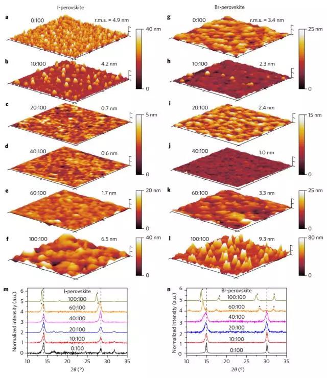
Organic-inorganic hybrid perovskite materials are becoming very attractive semiconductor materials for optoelectronics. In addition to their use in photovoltaics, perovskites are promising for use in light-emitting diodes (LEDs) due to their high color purity, low non-radiative recombination rate and adjustable bandgap. Xiao et al. reported high-efficiency perovskite LEDs formed using nano-sized microcrystalline self-assembly. The long chain ammonium halide added to the perovskite precursor solution acts as a surfactant, significantly limiting the growth of the 3D perovskite particles during film formation, resulting in crystallites having a size of 10 nm and a film roughness of less than 1 nm. Coating these nano-sized perovskite particles with longer chain organic cations produces a highly efficient emission source, resulting in an external quantum efficiency of 10.4% for the methylammonium iodide system, for methylammonium bromide system 9.3 % external quantum efficiency with significantly improved operational stability. (Nature PhotonicsDOI: 10.1038/NPHOTON.2016.269)
2. Warped two-dimensional unitene
(Buckled two-dimensional Xene sheets)
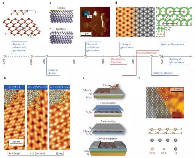
Silane, terpene, and tinnes are all part of a two-dimensional (2D) crystal of a singlet class (called two-dimensional X-ene, X = Si, Ge, Sn, etc.), which is similar to graphene but different The degree of warping of the IVA family of atomic cellular lattice arrangements. Their ligand functionalized derivatives are referred to as X-alkanes. Their electronic structure depends on the substrate, chemical functionalization and strain, ranging from simple insulators to semiconductors and semi-metals with adjustable gaps. A dozen different topological insulator states are expected, including quantum spin Hall states at room temperature, which, if implemented, will enable new types of nanoelectronics and spintronics (such as topological field effect transistors). For example, the electronic structure can be tuned by changing the IVA family element, spin-orbit coupling, functional chemistry, or substrate, making the two-dimensional X-ene system a promising multi-functional two-dimensional material for nanotechnology. (Nature Materials DOI: 10.1038/NMAT4802)
3. Optical-valley electron imaging of atomic-scale ultra-thin semiconductors
(Opto-valleytronic imaging of atomically thin semiconductors)
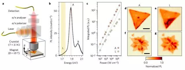
Transition metal disulfide semiconductors represent a fundamental component of layered heterostructures and have important applications in the latest technologies other than conventional optoelectronics. In a single layer form, they carry electrons with quantized circular motion and associated valley polarization and valley coherence as key elements of light-valley electron function. Neumann et al. introduced a two-dimensional polarimeter as a tool for direct imaging of the spine spine in a single-layer transition metal disulfide. Neumann et al. used MoS2 as a representative material for valley-selective optical transitions, established a polarization map of the extended crystal for quantitative image analysis, and used valley polarization and valley coherence as sensitive probes for crystal turbulence. In addition, they also found a site-dependent thermal and non-thermal mechanism for valley-polarized excitons in a vertical magnetic field. Finally, they demonstrated the potential of wide-area polarization measurements for rapid inspection of atomic-scale ultrathin semiconductors and heterostructured optoelectronic devices. (Nature Nanotechnology DOI: 10.1038/NNANO.2016.282)
4. Reasonable design of reconfigurable prismatic structural materials
(Rational design of reconfigurable prismatic architected materials)
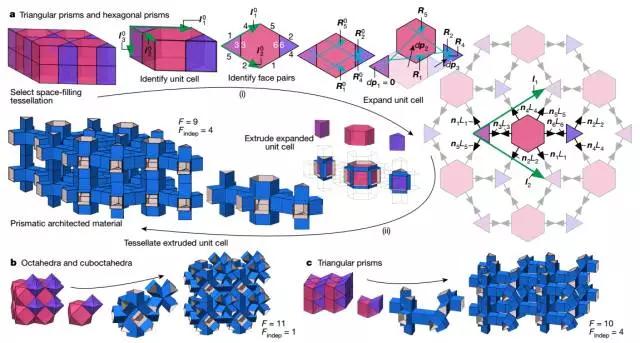
Advances in manufacturing technology have enabled the production of materials with unprecedented performance. Most such materials are characterized by a fixed geometry, but in some material designs, they can be combined with the inherent mechanisms that enable their spatial architecture to be reconstructed, and tunable functions are achieved in this manner. Inspired by the structural diversity and collapsibility of the prismatic geometry constructed by the polyline origami technique, Overvelde et al. introduced a polyhedral-based space-filled mosaic design strategy to create three-dimensional reconfigurable materials, including rigid slabs and elastic hinges. Periodic assembly. Through numerical analysis and physical prototype guidance, Overvelde et al. systematically explored the mobility of the design structure and determined various deformations and internal rearrangements of different qualities. Given that the fundamentals are scale-independent, the strategy can be applied to the design of next-generation reconfigurable structures and materials, ranging from variable-scale meters to nano-scale tunable subsystems. (Nature DOI: 10.1038/nature20824)
5. Carbon nanotube complementary transistor with gate length of 5 nm
(Scaling carbon nanotubecomplementary transistors to 5-nm gate lengths)
Qiu et al. reported a high performance top-gate carbon nanotube field effect transistor (CNT FET) with a gate length of 5 nm, which is better than a silicon complementary metal oxide semiconductor (CMOS) FET at the same scale. Scaling trend studies have shown that CNT-based devices using graphene contacts can operate faster at lower supply voltages (0.4 volts lower than 0.7 volts) and have much smaller subthreshold slopes ( Usually 73mV/Dec). The 5 nm CNT FET is close to the quantum limit of the FET, using only one electron per switching operation. In addition, the contact length of CNT CMOS devices is also reduced to 25 nm. Also, they showcased CMOS inverters with a total pitch of 240 nm. (Science DOI: 10.1126/science.aaj1628)
6. Conversion of bulk alloys to oxide nanowires
(Transformation of bulk alloys to oxidenanowires)
One-dimensional (1D) nanostructures provide a good choice for enhancing the electrical, thermal, and mechanical properties of functional materials and composites, but their synthesis is often complex and expensive. Lei et al. demonstrated the direct conversion of bulk materials into nanowires under environmental conditions without the use of catalysts or any external stimuli. Nanowires are formed by minimizing the strain energy at the boundary of the chemical reaction front. Lei et al. demonstrated that a plurality of sized particles of aluminum or magnesium alloys are converted into a sized alkoxide nanowires that are further converted to oxide nanowires when heated in air. The separator based on alumina nanowires improves the safety and rate performance of lithium ion batteries. Their approach enables ultra-low cost scalable synthesis of one-dimensional materials and membranes. (Science DOI: 10.1126/science.aal2239)
7. Mechanical behavior and design of lightweight three-dimensional graphene assembly
(The mechanics and design of alightweight three-dimensional graphene assembly)

Studies on three-dimensional graphene assemblies have demonstrated solid porous materials that are lighter than air. Due to its strong mechanical properties, this solid-state material can be used under extreme conditions, for example as a substitute for crucibles in flying balloons. However, little is known about the elastic modulus and strength of porous graphene assemblies, which hinders the evaluation of the feasibility of their application. Qin et al. combined the bottom-up computational simulation with 3D-printing-based model experiments to study the mechanical behavior of porous 3D graphene. Although 3D graphene has extremely high strength at relatively high density, its mechanical properties rapidly decrease with increasing density, and are faster than polymer foam. Their results give the critical density of the 3D graphene assembly, below which it begins to lose its mechanical properties. (ScienceAdvances DOI: 10.1126/sciadv.1601536)
8. Application of two-dimensional carbides and nitrides (MXenes) in energy storage
(2D metal carbides and nitrides (MXenes) for energy storage)
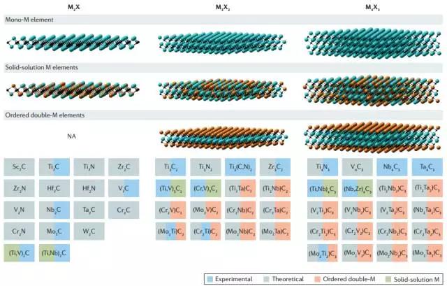
Two-dimensional transition metal carbides, carbonitrides and nitrides (collectively MXenes) have been rapidly expanded from the 2011 Ti3C2. These materials always have surface passivation, such as hydroxyl, oxygen or fluorine, which imparts superhydrophilicity to the surface. About 20 different MXenes have been synthesized, and more than a dozen structures and properties have been theoretically predicted. The availability of these solid solutions, the controllability of passivation and the recent discovery of multi-transition metal layered MXenes offer opportunities and possibilities for the synthesis of many new structures. Mxenes' diverse chemistry allows it to be used in energy storage, electromagnetic interference shielding, composite strengthening, water treatment, sensors, lubrication and photoelectrochemical catalysis. Gogotsi et al. reviewed the synthesis, structure and properties of MXenes and their applications in energy storage and related applications. (Nature Reviews Materials, DOI:10.1038/natrevmats.2016.98)
An intermediate is the reaction product of each of these steps, except for the last one, which forms the final product.
Our Veterinary Intermediate products are manufactured with professional technic and standard process which is also widely used as a kind of main materials of Veterinary drugs.
The Veterinary intermediate can be used to manufacture many products including Insecticide, Bactericide, and ect.
Veterinary Intermediate
Veterinary Intermediate,Veterinary Drug,Veterinary Drug Intermediates
Hebei Senton International Trading Co.,Ltd. , https://www.sentonpharm.com

